Rev. 2.01 9/01
Copyright © 2001 by Silicon Laboratories
Si3038-DS201
Si3038
G
L O B A L
MC'97 S
I L I C O N
DAA
Features
Complete DAA includes:
Applications
Description
The Si3038 is an integrated direct access arrangement (DAA) chipset that
provides a digital, programmable line interface to meet global telephone
line requirements. Available in two 16-pin small outline packages (AC'97
interface on Si3024 and phone-line interface on Si3014), the chipset
eliminates the need for an analog front end (AFE), an isolation
transformer, relays, opto-isolators, and a 2- to 4-wire hybrid. The Si3038
dramatically reduces the number of discrete components and cost
required to achieve compliance with global regulatory requirements. The
Si3024 complies with the AC'97 2.1 specification.
Functional Block Diagram
AC'97 2.1 Compliant
Primary or Secondary Codec
Global Phone Line Interface
Compliant with FCC, CTR21,
JATE, and Other PTTs
84 dB Dynamic Range TX/RX
Paths
3.3 V or 5 V Power Supply
Greater than 3000 V Isolation
Integrated Ring Detector
Wake-Up On Ring
Caller ID Support
Integrated Analog Front End
2- to 4-Wire Hybrid
Low-Power Standby Mode
Low Profile SOIC Packages
Patented ISOcapTM Technology
Software Modems
Audio/Telephony Sub-Systems
Audio/Modem Riser Cards (AMR)
Mobile Daughter Cards (MDC)
Mini-PCI Cards
Si3024
Clock
Control
Interface
Isolation
Interface
XOUT
MCLK/XIN
BIT_CLK
SYNC
GPIO_A
GPIO_B
RESET
SDATA_IN
AC'97
Digital
Interface
SDATA_OUT
ID0
ID1
Hybrid
and
DC
Termination
Ring Detect
Off-Hook
FILT
FILT2
REF
DCT
VREG2
REXT
REXT2
RNG1
RNG2
QB
QE
QE2
RX
Si3014
Isolation
Interface
VREG
US Patent # 5,870,046
US Patent # 6,061,009
Other Patents Pending
Ordering Information:
See page 59.
Pin Assignments
Si3024 (SOIC)
Si3024 (TSSOP)
Si3014 (SOIC or TSSOP)
1
16
2
15
3
14
4
13
5
12
6
11
7
10
8
9
GPIO_A
ID1
V
A
GND
C1A
ID0
A OUT
GPIO_B
MCLK/XIN
XOUT
BIT_CLK
SDA TA _IN
SY NC
SDA TA _OUT
RESET
V
D
1
16
2
15
3
14
4
13
5
12
6
11
7
10
8
9
V
D
XOUT
MCLK/XIN
GPIO_A
GPIO_B
ID1
V
A
BIT_CLK
SDA TA _IN
SDA TA _OUT
SY NC
A OUT
C1A
ID0
GND
RESET
1
16
2
15
3
14
4
13
5
12
6
11
7
10
8
9
QE2
DCT
IGND
RNG1
QB
RNG2
QE
C1B
FILT2
RX
REXT
REXT2
REF
V REG2
V REG
FILT

Si3038
Rev. 2.01
3
T
A B L E
O F
C
O N T E N TS
Section
Page
Electrical Specifications . . . . . . . . . . . . . . . . . . . . . . . . . . . . . . . . . . . . . . . . . . . . . . . . . 4
Typical Application Circuit . . . . . . . . . . . . . . . . . . . . . . . . . . . . . . . . . . . . . . . . . . . . . . . 16
Bill of Materials . . . . . . . . . . . . . . . . . . . . . . . . . . . . . . . . . . . . . . . . . . . . . . . . . . . . . . . . . 17
Analog Output . . . . . . . . . . . . . . . . . . . . . . . . . . . . . . . . . . . . . . . . . . . . . . . . . . . . . . . . . 19
Functional Description . . . . . . . . . . . . . . . . . . . . . . . . . . . . . . . . . . . . . . . . . . . . . . . . . . 20
Initialization . . . . . . . . . . . . . . . . . . . . . . . . . . . . . . . . . . . . . . . . . . . . . . . . . . . . . . . . 22
AC-Link . . . . . . . . . . . . . . . . . . . . . . . . . . . . . . . . . . . . . . . . . . . . . . . . . . . . . . . . . . . 22
Isolation Barrier . . . . . . . . . . . . . . . . . . . . . . . . . . . . . . . . . . . . . . . . . . . . . . . . . . . . . 22
Off-Hook . . . . . . . . . . . . . . . . . . . . . . . . . . . . . . . . . . . . . . . . . . . . . . . . . . . . . . . . . . . 23
DC Termination . . . . . . . . . . . . . . . . . . . . . . . . . . . . . . . . . . . . . . . . . . . . . . . . . . . . . 23
DC Termination Considerations . . . . . . . . . . . . . . . . . . . . . . . . . . . . . . . . . . . . . . . . . 24
AC Termination . . . . . . . . . . . . . . . . . . . . . . . . . . . . . . . . . . . . . . . . . . . . . . . . . . . . . 24
Ring Detection . . . . . . . . . . . . . . . . . . . . . . . . . . . . . . . . . . . . . . . . . . . . . . . . . . . . . . 24
Ringer Impedance . . . . . . . . . . . . . . . . . . . . . . . . . . . . . . . . . . . . . . . . . . . . . . . . . . . 25
Wake-Up on Ring . . . . . . . . . . . . . . . . . . . . . . . . . . . . . . . . . . . . . . . . . . . . . . . . . . . . 25
DTMF Dialing . . . . . . . . . . . . . . . . . . . . . . . . . . . . . . . . . . . . . . . . . . . . . . . . . . . . . . . 26
Pulse Dialing . . . . . . . . . . . . . . . . . . . . . . . . . . . . . . . . . . . . . . . . . . . . . . . . . . . . . . . 26
Billing Tone Detection . . . . . . . . . . . . . . . . . . . . . . . . . . . . . . . . . . . . . . . . . . . . . . . . 26
Billing Tone Filter (Optional) . . . . . . . . . . . . . . . . . . . . . . . . . . . . . . . . . . . . . . . . . . . . 27
On-Hook Line Monitor . . . . . . . . . . . . . . . . . . . . . . . . . . . . . . . . . . . . . . . . . . . . . . . . 28
Caller ID . . . . . . . . . . . . . . . . . . . . . . . . . . . . . . . . . . . . . . . . . . . . . . . . . . . . . . . . . . . 28
Loop Current Monitor . . . . . . . . . . . . . . . . . . . . . . . . . . . . . . . . . . . . . . . . . . . . . . . . . 28
Overload Detection . . . . . . . . . . . . . . . . . . . . . . . . . . . . . . . . . . . . . . . . . . . . . . . . . . 29
Analog Output . . . . . . . . . . . . . . . . . . . . . . . . . . . . . . . . . . . . . . . . . . . . . . . . . . . . . . 29
Gain Control . . . . . . . . . . . . . . . . . . . . . . . . . . . . . . . . . . . . . . . . . . . . . . . . . . . . . . . . 29
Filter Selection . . . . . . . . . . . . . . . . . . . . . . . . . . . . . . . . . . . . . . . . . . . . . . . . . . . . . . 29
In-Circuit Testing . . . . . . . . . . . . . . . . . . . . . . . . . . . . . . . . . . . . . . . . . . . . . . . . . . . . 29
Digital Interface . . . . . . . . . . . . . . . . . . . . . . . . . . . . . . . . . . . . . . . . . . . . . . . . . . . . . . . . 30
Si3024 as Secondary Device . . . . . . . . . . . . . . . . . . . . . . . . . . . . . . . . . . . . . . . . . . . 30
Si3024 as Primary MC'97 Codec . . . . . . . . . . . . . . . . . . . . . . . . . . . . . . . . . . . . . . . . 30
Si3024 Connection to the Digital AC'97 controller . . . . . . . . . . . . . . . . . . . . . . . . . . . 30
Clocking . . . . . . . . . . . . . . . . . . . . . . . . . . . . . . . . . . . . . . . . . . . . . . . . . . . . . . . . . . . 30
Resetting Si3038 Chipset . . . . . . . . . . . . . . . . . . . . . . . . . . . . . . . . . . . . . . . . . . . . . . 30
AC-Link Digital Serial Interface Protocol . . . . . . . . . . . . . . . . . . . . . . . . . . . . . . . . . . 31
Codec Register Access . . . . . . . . . . . . . . . . . . . . . . . . . . . . . . . . . . . . . . . . . . . . . . . 36
AC-Link Low Power Mode . . . . . . . . . . . . . . . . . . . . . . . . . . . . . . . . . . . . . . . . . . . . . 37
Control Registers . . . . . . . . . . . . . . . . . . . . . . . . . . . . . . . . . . . . . . . . . . . . . . . . . . . . . . . 38
Appendix A--UL1950 3rd Edition . . . . . . . . . . . . . . . . . . . . . . . . . . . . . . . . . . . . . . . . . . 53
Appendix B--CISPR22 Compliance . . . . . . . . . . . . . . . . . . . . . . . . . . . . . . . . . . . . . . . . 54
Pin Descriptions: Si3024 . . . . . . . . . . . . . . . . . . . . . . . . . . . . . . . . . . . . . . . . . . . . . . . . . 55
Pin Descriptions--Si3014 . . . . . . . . . . . . . . . . . . . . . . . . . . . . . . . . . . . . . . . . . . . . . . . . 57
Ordering Guide . . . . . . . . . . . . . . . . . . . . . . . . . . . . . . . . . . . . . . . . . . . . . . . . . . . . . . . . . 59
SOIC Outline . . . . . . . . . . . . . . . . . . . . . . . . . . . . . . . . . . . . . . . . . . . . . . . . . . . . . . . . . . . 60
TSSOP Outline . . . . . . . . . . . . . . . . . . . . . . . . . . . . . . . . . . . . . . . . . . . . . . . . . . . . . . . . . 61
Contact Information . . . . . . . . . . . . . . . . . . . . . . . . . . . . . . . . . . . . . . . . . . . . . . . . . . . . . 64
Si3038
4
Rev. 2.01
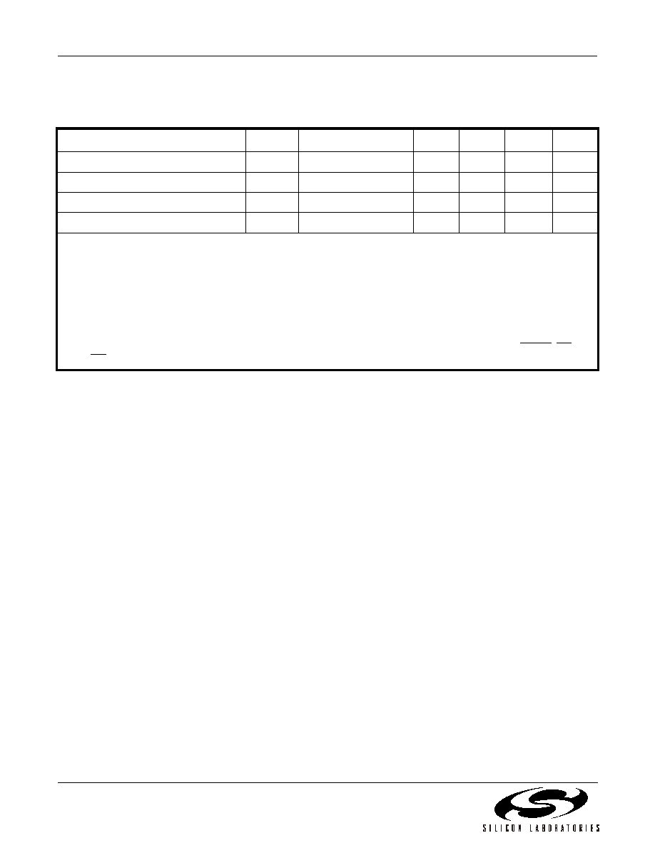
Electrical Specifications
Table 1. Recommended Operating Conditions
Parameter
1
Symbol
Test Condition
Min
2
Typ
Max
2
Unit
Ambient Temperature
3
T
A
K-Grade
0
25
70
∞C
Si3024 Supply Voltage, Analog
V
A
4.75
5.0
5.25
V
Si3024 Supply Voltage, Digital
4
V
D
V
A
= 5 V
4.75
5.0
5.25
V
Si3024 Supply Voltage, Digital
4
V
D
V
A
= Charge Pump
3.0
3.3
3.6
V
Notes:
1. The Si3038 specifications are guaranteed when the typical application circuit (including component tolerances) of
Figure 19 on page 16 and any Si3024 and Si3014 are used.
2. All minimum and maximum specifications are guaranteed and apply across the recommended operating conditions.
Typical values apply at nominal supply voltages and an operating temperature of 25∞C unless otherwise stated.
3. The temperature specifications are guaranteed when using the typical application circuit on a 4 sq. in. minimum FR4
PCB. For other materials and smaller form factors, heat dissipation factors may apply. Contact Silicon Laboratories for
more details.
4. The digital supply, V
D,
can operate from either 3.3 V or 5.0 V. The Si3024 supports interface to 3.3 V logic when
operating from 3.3 V. 3.3 V operation applies to both the AC'97 Digital Interface and the digital signals RESET, ID0, and
ID1.